Dan Barlow's Webpage
Arduino MEGA 2560 Sub Layer Access Breakout > In development <
Back to ShieldsWhile working on the memory expansion boards, I encountered supply problems with the stacking headers. The 36 pin dual row stacking header for the external memory interface was not available in quantity at a reasonable price.
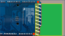
A circuit board could be placed below the Arduino board and connected by soldering through to the existing pin socket stubs. The fillets would prevent direct contact between the boards, but the stubs are tall enough to register with another board and solder would make the electrical and mechanical connection.

The MEGA's mounting holes will limit the board size and the board edge overlay will constrain the placement of parts near the connection.
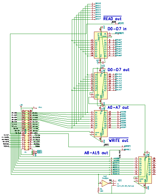 |
The Access Breakout must at at minimum provide the address latch to demultiplex address lines 0 to 7. In thinking about what other functions it should support, I'm keeping in mind that the Atmega 2560 has a limit on how long a trace it can drive and how many loads it can handle. One way to address this is to use transparent latches as buffers, to repeat the signal and protect the main chip from interference. The AHC logic series have the ability to receive 5 volt signals while operating on 3.3 volts without damage. An option is to provide a separate trace for the power supply of all outgoing buffers, so the output will be 3.3V compatible if this is connected to 3.3V and 5V compatible if it is connected to 5V. See this discussion of logic level compatibility. It is one of my regular battles to stop optimizing for all possibilities and just finish a thing, so Plan A is to impletement a fully 5 Volt system. The next consideration is the sourcing of the Output Enable signal for the inbound data latch. This signal needs to be generated during a read so the latch drives the data lines. If there is also a memory or another possible data source on the data lines, the output enable must only be driven when its memory address (or range) is selected. The usual answer to this is an address decoder. There are several methods used, and I explored both the multi input NAND gate and the Identity Detector logic chips. The Identity Detector is designed for cascading and doesn't need inverters, so the layout is much smaller. I'm considering doing one based on the 13 input NAND and a 16 bit inverting buffer. The timing of each approach is within spec for this application.   The next consideration is the size of the memory mapped I/O region. The address decoders above decode 15 or 16 bits of address, creating 2 or 1 ports. Address decoder lectures usually discuss the 3 to 8 or 4 to 16 decoders to process the lower bits of the address, and I do want to have a significant number of ports for DACs. The 74HC154 4 to 16 decoder at 5V specifies an 11 nS response time for both address and enable changes. This device includes two active-low output enables so it can decode high address /DETECT and /READ or /WRITE. Specifying it means that the address decoder needs to process 12 bits. |
Those decisions mean the second identity detector is half used and the other half of the inputs can be ground.
The upper 8 bit identity comparator output can be routed to additional lower detectors for more pages in the I/O block.
For the first draft, only one input and one output latch are placed.
